Gates: EXTENSION
|
Extension : Uses of gates This section is provided to extend your knowledge above and beyond that which is required for the A-Level course. The concepts here are not easy but you might find them interesting and if you choose to study Computer Science at uni, the material here should come in useful.
|
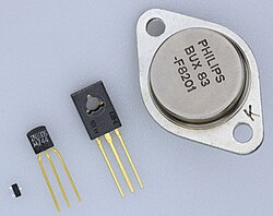
Almost all modern digital electronics is made using "CMOS". Earlier valve, DTL (Diode-Transistor Logic) and TTL (Transistor-Transistor Logic) are of historical interest but now used for special purposes only (TTL signalling levels are often used with CMOS logic which can result in confusion).

The name CMOS is an amalgam of "C" for Complementary and the "MOS" of MOSFET (Metal Oxide Semiconductor Field Effect Transistor). MOS comes from the original construction as a metal (aluminium) gate on a layer of oxide (Silicon Dioxide) insulation on top of a semiconductor (or Silicon) base. Polysilicon is now used instead of metal because it is easier to make but metal is coming back in the very latest designs. Similarly better materials than Oxide are used in the latest designs.
MOSFET devices come in two variants, n-type (NMOS) and p-type (PMOS) depending on the doping agent added to the semiconductor base. CMOS uses pairs of one NMOS and one PMOS transistors with typically the same input connected to the NMOS gate and the PMOS gate and the drain and source in series. Only one transistor conducts at once, minimizing the power drain.
| Name | PMOS transistor | NMOS transistor |
|---|---|---|
| Diagram | ||
| conducts when input is: | low (0) | high (1) |
The advantage of CMOS is that because the gate is insulated and the drivers complementary (so one is on and one off) there is minimal leakage current except when the gate is actively switching. Indeed where CMOS is driving CMOS, the static current is practically negligible. On any large integrated circuit only a small percentage of the gates will be switching at any one time and the rest static. So only the active gates consume power and only for the short switching period. This also explains why the power usage (and thus heating) of modern CPU chips is proportional to the clock speed.
The basic inverter circuit (NOT gate) looks like this:

The upper gate is a PMOS transistor which conducts only when A is low voltage (near Vss, the source voltage) and the lower gate is NMOS which conducts only when A is high voltage (near Vdd, the drain voltage). The output Q is thus forced to Vdd when A is near Vss and vice-versa. In addition the voltage change in A (with minimal current) can produce a significant current supply in Q. Normally Vdd is in the range +2v to +5v and regarded as a logic "1" whereas Vss is 0v and regarded as a logic "0".
Note that if the input A came from an external switch or similar then a pull-up or pull-down resistor would be required so that when the switch was open A would take a definite value and not float (take on an indeterminate value). The switch would connect A to the opposite rail. If A came from an external source then diodes would be added to ensure that A takes values only between Vss and Vdd.
The basic two input NAND gate looks like this:

Here the bottom part of the circuit pulls down only if both A and B are high (opening the two bottom transistors) and the upper part pulls up if either are low. This pattern can be extended to three or four inputs with ease allowing for gates with more than two inputs. In practice, an inverter needs to be added to the output to make the gate perform correctly. Thus the most basic gate is an AND:

A second inverter is added to the gate above to get a NAND function. A CMOS NOR circuit is just the mirror of the NAND.
|
CMOS OR Gate
|
Practical CMOS XOR gates actively use the A and B inputs instead of Vss and Vdd to reduce the number of gates and are beyond the scope here. In real life you would take a standard design; but it is possible to create a XOR gate out of other CMOS gates, using the following identity we could theoretically make a CMOS XOR out of an OR ANDed with a NAND:
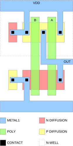
A physical CMOS NAND (without inverter) looks like this:

More complex examples
[edit | edit source]Flip Flop
[edit | edit source]A one bit memory is called a flip-flop. These are used for CPU registers such as the MAR (but not for bulk memory as they take up a lot of physical space and RAM chips would be infeasibly big). One of the simplest is called a JK flip-flop:

The two NOR gates form the memory; at any one time one is high, the other low and feedback maintains that state. A J high pulse causes the top NOR to go off and a 1 to be stored (Q is high) and a K high pulse causes the bottom NOR to go off and a 0 to be stored (Q is low). (If both J and K pulse together the output changes state.) Real world devices would have input conditioning, output inverters and often additional set, reset and clock inputs.
Adders
[edit | edit source]You may have met the following logic circuit before:

If we take a look at the truth table:
| A | B | C | S |
|---|---|---|---|
| 0 | 0 | 0 | 0 |
| 0 | 1 | 0 | 1 |
| 1 | 0 | 0 | 1 |
| 1 | 1 | 1 | 0 |
You may be able to tell, what the above circuit does is allows you to add the two inputs, A and B, together:
 B
+A
--
CS
This is great and called a half-adder, but it only manages to add two 1 bit digits together. What is needed is a full-adder. A more complex circuit is a one bit adder that take into account any carry brought over from a previous calculation:

This device allows you to string the one bit adders together, creating a multiple bit adder (in this case 4 bit):

In producing a multi-bit adder, the A and B are inputs for each bit and S the respective sum output bits. The Cin comes from the next lower bit and the Cout goes to the next higher bit or to the overflow detection logic (which checks when a result is too big to fit into all the S outputs). In practical designs carry look ahead is done 4, 8 or more bits at a time to avoid the ripple delay of carry propagation (the time taken for the carry bits to filter through from the first calculation to a calculation several steps down). In real ALUs (arithmetic logic units) additional inputs select the function to be done (add, subtract, and, or, etc.) so that a general purpose unit for all simple bitwise functions is created.
FPGAs and ASICs
[edit | edit source]The days of individual logic elements connected by wire or PCB tracks are long gone. A typical modern design uses a few basic building blocks such as memory, CPU and Ethernet interfaces (which are off the shelf) and mops up the remaining design into a few large chips which contain many individual logic elements.
The ability to put many millions of transistors on a single chip means that designing a chip for one purpose is a very expensive and time consuming process. It can be justified only for chips that will sell in very large volumes (like desktop and laptop computers or industrial controllers that will be used in a range of products). Two approaches are used for smaller volume chips. A Field Programmable Gate Array (FPGA) is a chip that contains blocks of logic and memory that determines how the blocks are interconnected. Sometimes the memory is permanent (but re-writable) although more frequently it is dynamic and loaded from a Flash chip external to the device during the power up sequence. Occasionally it is loaded by a CPU. Originally the logic blocks were simple functions (flip-flops, adders, AND gates etc.) but in modern FPGAs they can include whole CPUs, RAM areas and similar features as well as basic logic functions. The terms CPLD (Complex Programmable Logic Device) and PAL/PLA (Programmable Array Logic/ Programmable Logic Array) are similar but used for smaller devices.
An application-specific integrated circuit (ASIC) is similar to an FPGA except that the chip is part fabricated as a standard design with logic blocks and then the last few layers of metal interconnect are added to the customer specification. This is cheaper than a custom designed chip but it can still cost millions of dollars to produce the masks and prototypes. It does produce a faster and more compact result than an FPGA so there are some designs that can only be done on an ASIC.
ASICs also have a cheaper unit cost, but FPGAs have advanced to the point where they are used in production not just for prototyping. The cost of a mistake in an ASIC is substantial whereas an FPGA can be upgraded in the field. ASICs are harder to copy than FPGAs and so are used in some applications requiring secrecy or security.
For both ASIC and FPGA designs the manufacturer provides software that translates a logic design into a layout for the device and enables simulation of the operation. There are also non-manufacturer specific tools and in particular a language called VHDL which can be used to describe a logic system and simulate it. Manufacturers then provide tools to produce the ASIC or FPGA design (often free). VHDL stands for “VHSIC hardware description language” and VHSIC stands for very high speed integrated circuits.


