Semiconductors/PN Junctions
Simple Models
[edit | edit source]These simple models are small signal approximations to how a fairly generic diode works. Zener and tunnel diodes are ignored.
At a first approximation, a diode is a device that will let current flow in one direction with zero resistance and will block current in the other direction with infinite resistance. Basically, it operates like a check valve for current.
A second approximation includes a constant voltage drop for current flow in the forward direction. The voltage drop varies with the type of diode, but is typically around 0.7 volts for fairly generic diodes and well over 1 volt for LEDs.
To get a third approximation, add a little resistance to the diode. Now things get a little more complicated. Since the v-i curve is non-linear, the resistance is not constant. However, if your signal is small and carried on a large offset, you can do a fairly accurate analysis by properly selecting the voltage drop and resistance.
Finally the fourth approximation accounts for the small leakage current that exists when the diode is reverse biased. This is typically in the range of nano-amps to a few micro-amps for most generic diodes.
If you need more accuracy than this, you will need to look at the physics that happens inside a diode.
Analysis of Diode Physics
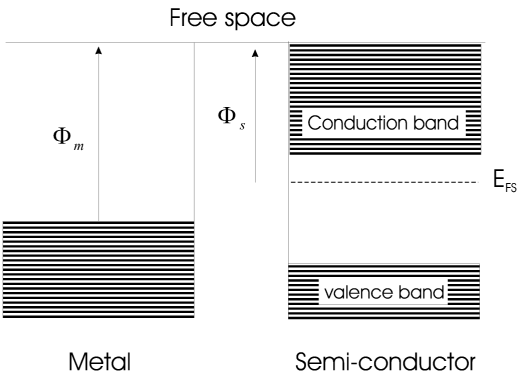
[edit | edit source]Diodes junctions may be formed with N type and P type semi-conductor or semi-conductor and Metal junction.
as .

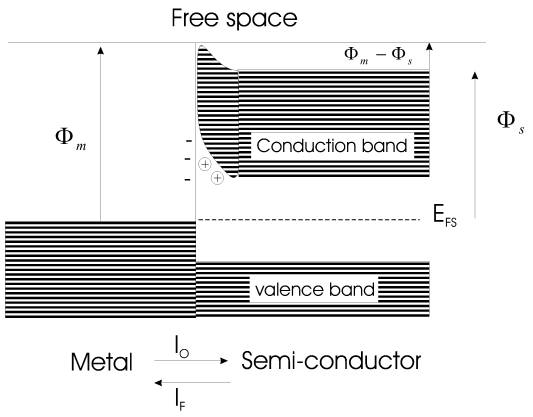
When the Metal and Semi-conductor come together, excess electrons diffuse from the semi-conductor to the metal until the Fermi levels are equal. As electrons diffuse from the semi-conductor to the metal, they leave behind their donor atom. This depletes the region near the interface of charge carriers and hence this region does not conduct well. Thus for charges to diffuse across this region, they require additional energy. Since the extent of the depletion of charges is some function of distance, the conduction band is bent to represent the energy required for diffusion in that region.

There will now exist 2 currents. Electrons diffuse from metal to semi-conductor over the barrier induced by the depletion region . Electrons diffuse from the semi-conductor over this barrier in the opposite direction . When there is no external applied voltage, there current will be equal and opposite.
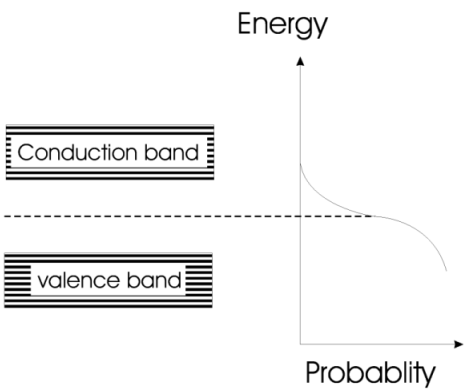
Electrons will diffuse from semi-conductor to metal if they have enough energy to overcome the barrier. The energy of an electron is statistical, and is given by the Maxwell-Boltzmann distribution [1]. Thus as the temperature increases, the probability of the number of electrons occupying higher energy states increases. For low doping densities, the Maxwell-Boltzmann distribution may also be applied. However for non-zero temperature most excess electrons from the dopant will exist in the conduction band.
Maxwell-Boltzmann distribution says: given an energy W, the number of electrons with energy greater than W is given by:
where n is the number density of electrons, k Boltzmann's constant and T the temperature.

The Maxwell-Boltzmann distribution does not apply to metals. The reason may be found in the referenced [1]. For small voltages one may assume to be constant.
for no external potential. This equilibrium exists for a diffusion potential we will call , where . Thus the energy of an electron to cross this barrier is given by .
The fermi level of the n-type semi-conductor may be increased by an external potential. This will increase the number of electrons with energy to diffuse across the barrier. Thus the energy for electron to cross the barrier will become .
Thus:
Let:
Then:
Depletion Width
[edit | edit source]The depletion width is given by the required amount of charge to be displaced to realize the diffusion potential. Thus if one knows the doping density and relative permittivity of the material, then one may calculate the depletion width.

The depletion width is easiest realized by Poisson's Equation [1]. Assume constant doping density.
By Poisson's equation:
where the charge density, the permittivity and x the distance from the junction.
The depletion width is some function of barrier height, . Therefore solve for
Depletion capacitance
[edit | edit source]Capacitance is the change in charge for change in voltage over the depletion width.
Given:
Then:
Let:
Therefore:
References
[edit | edit source][1] John Allison. Electronic Engineering Semiconductors and devices. McGraw-Hill Book Company, Shoppenhangers Rd Maidenhead Berkshire England,1971.


